How High Frequency PCB work
2025-05-29
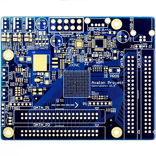
High-frequency PCBs (Printed Circuit Boards) are designed to handle signals with high frequencies—typically above 500 MHz, and often reaching into the GHz range. These are used in applications like RF (radio frequency), microwave circuits, high-speed digital circuits, and radar systems.
Here’s how high-frequency PCBs work and what makes them different from standard PCBs:
1. Specialized Materials
High-frequency signals are more sensitive to losses and interference, so standard FR4 (used in typical PCBs) doesn’t work well. Instead, low-loss dielectric materials are used:
PTFE (Teflon)
Ceramic-filled PTFE
Rogers materials (like RO4003C, RO4350B)
Hydrocarbon ceramic
These materials have:
Low dielectric constant (Dk) for consistent signal speed
Low dissipation factor (Df) for minimal signal loss
Stable thermal properties
2. Impedance Control
High-frequency PCBs require precise impedance matching to prevent signal reflections and distortion. Designers tightly control:
Trace width
Spacing
Dielectric thickness
Ground plane structure
Transmission lines like microstrip and stripline are used to carry high-frequency signals while controlling impedance.
3. Signal Integrity Management
At high frequencies, even tiny issues can distort signals. Design considerations include:
Minimized crosstalk between traces
Short, direct signal paths
Use of ground planes to return current paths cleanly
Via and connector design to minimize parasitics

4. Multilayer Stack-ups
High-frequency PCBs are often multilayered to allow:
Power and ground planes for shielding
Controlled impedance routing layers
Isolation between analog and digital signals
5. Manufacturing Precision
Fabrication must be precise:
Tight etching tolerances
Careful lamination processes
Consistent material thickness
Manufacturers of high-frequency PCBs specialize in tight controls and testing.
If you are interested in our products or have any questions, please feel free to contact us and we will reply you within 24 hours.


